Our
Services
Components Design
and Library Management
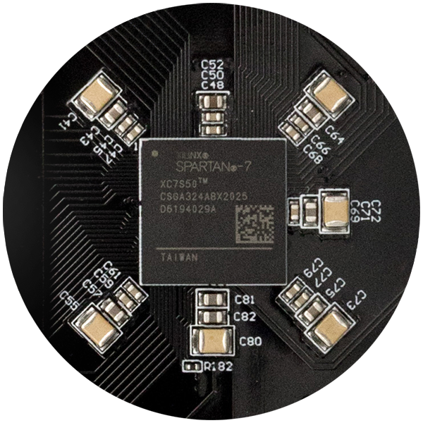
For every electronic product, the cost management starts with component selection. We are entirely flexible, and for a successful design, we could select and validate the electronic parts, or we could work closely with you to integrate the ones you preferred. At Keytek, we create and manage all the components and the library, considering a rigorous internal procedure verification.
Schematic design
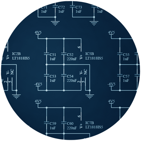
Today’s competitive market needs cost-effective and reliable products. At Keytek, we have experience in a wide variety of product circuit designs with varying complexity – from simple circuits to complex embedded projects. To turn the ideas into a circuit design quickly, we use tools from the leading technology manufacturer to draw the detailed schematic, simulated the critical block, and calculated the key parameters using different analytical methods.
PCB Layout Design
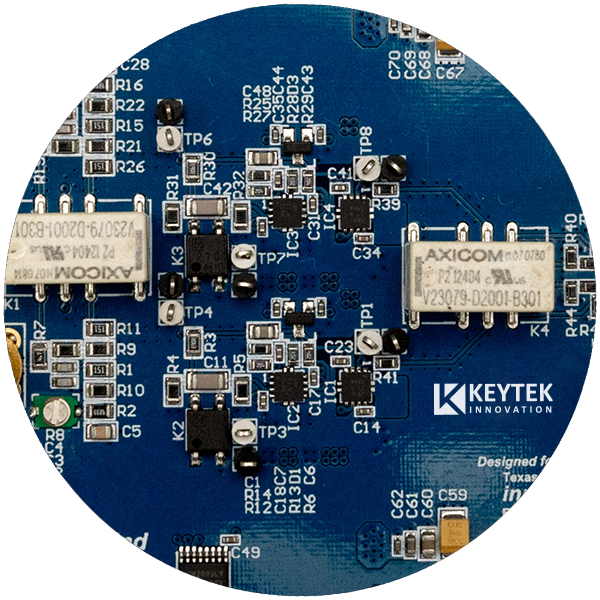
Modern PCB layout design is a complex process with many considerations and almost all the time with no single “right” answer to achieving the desired outcome. The analytical skills, combined signal/power integrity simulations, and an in-depth understanding of the PCB design process will generate the best design choices to balance the price/performance ratio. Our experienced and skilled Electronic Design Engineer could handle from simple two layers PCB boards to the most demanding technology designs. At Keytek, we have vast experience with HDI PCB design and layout design constraints for high-speed interfaces, power distributions networks, or RF designs. We could support you with the PCB layout design from schematic to fabrication, or we could assist you in the artwork of the most critical blocks.
Validation and Verification
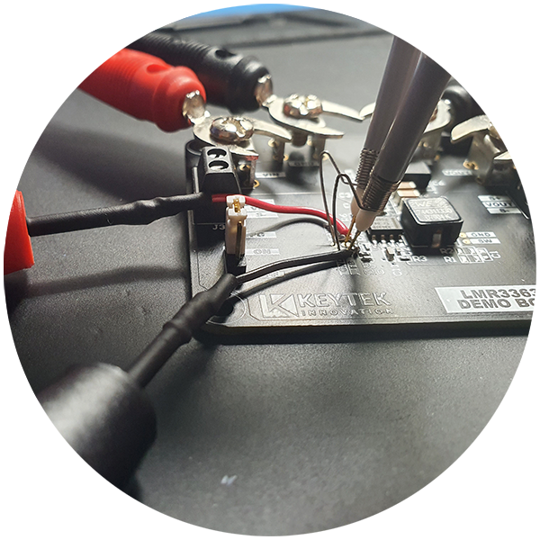
Ensuring consistency, repeatability and reproducibility are the main goals when we perform system validation and verification. To guarantee this, we use measurement instruments from industry-leading companies and post-processed the results using different programming languages. A detailed report with measurement setup, results, and necessary schematic and PCB layout improvements complete the testing process.
Simulation
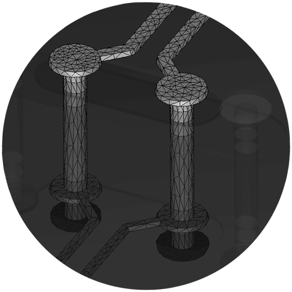
In today’s fast-paced digital world, where new standards bring higher data rates and more complex designs, the process design must adapt. To reduce the debugging time, decrease layout iteration, and ensure product performance, the design process should include a comprehensive suite of analysis and verification techniques from the earliest design stage. At Keytek, we use high-performance 3D EM analysis software and circuit simulation to perform signal and power integrity simulations. A detailed report with system requirements, simulation results, and necessary layout guidelines completes the analysis.
Contact
us
Terms & Conditions Privacy Policy
Copyright 2020 - By Keytek Innovation
